Probe Card Manufacturing Process in California
Probe cards are critical components in the semiconductor manufacturing industry, serving as interfaces between the electronic testing equipment and the semiconductor wafer. California, being a hub of technological innovation and home to Silicon Valley, plays a pivotal role in the development and production of high-quality probe cards. The manufacturing process of probe cards in California is a complex and meticulous procedure involving several stages, from design to final testing, ensuring the precision and reliability required for semiconductor testing.
Probe Card Manufacturing of Design and Development
Initial Concept and Requirements
The manufacturing process begins with the design and development phase, where the initial concept of the probe card is created based on specific requirements. These requirements are dictated by the type of semiconductor device being tested, the testing parameters, and the testing environment. Engineers collaborate closely with clients to understand their needs, which includes the number of probes, the type of probes (cantilever, vertical, membrane, etc.), and the precise layout of the semiconductor wafer.
CAD Modeling and Simulation
Once the requirements are gathered, engineers use Computer-Aided Design (CAD) software to create detailed models of the probe card. These models help in visualizing the physical layout and ensuring that all components fit together perfectly. Simulations are then run to predict the performance of the probe card under various conditions. These simulations are crucial as they help in identifying potential issues and optimizing the design before moving to the prototyping stage.
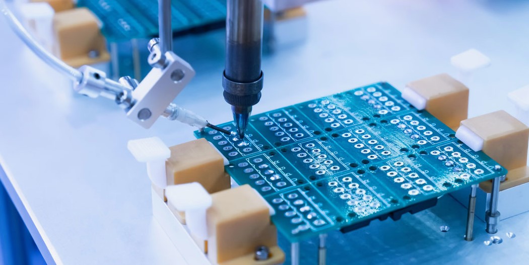
Prototyping and Fabrication
Material Selection
The next step involves selecting the appropriate materials for the probe card. The choice of materials is critical as it affects the durability, electrical conductivity, and overall performance of the probe card. Common materials used include tungsten, beryllium copper, and various types of ceramics. The selection process also takes into account the manufacturing techniques that will be used, ensuring compatibility and ease of fabrication.
Prototype Development
With the design finalized and materials selected, the prototype development begins. This stage involves the actual fabrication of the probe card using advanced manufacturing techniques such as photolithography, precision machining, and electroforming. These techniques allow for the creation of intricate and precise components that are essential for the functionality of the probe card.
Assembly and Testing
Component Assembly
Once the individual components are fabricated, the next step is to assemble them into a complete probe card. This assembly process requires high precision and attention to detail, as any misalignment or defect can significantly affect the performance. Technicians use specialized equipment to align and secure the probes, ensuring they make perfect contact with the semiconductor wafer during testing.
Initial Testing
After assembly, the probe card undergoes initial testing to check for electrical continuity, mechanical integrity, and overall functionality. This initial testing helps identify any defects or issues that need to be addressed before the final testing stage. Engineers use sophisticated testing equipment to simulate the actual testing environment and verify the performance of the probe card.
Final Testing and Quality Assurance
Performance Testing
In the final testing phase, the probe card is subjected to rigorous performance tests to ensure it meets all specifications and requirements. These tests include electrical performance tests, mechanical stress tests, and thermal cycling tests. The goal is to ensure that the probe card can reliably and accurately test the semiconductor devices under real-world conditions.
Quality Assurance
Quality assurance is a critical part of the manufacturing process. Each probe card undergoes thorough inspection and testing to ensure it meets the highest standards of quality and reliability. This involves both automated and manual inspections to check for any defects or inconsistencies. Only after passing these stringent quality checks is the probe card deemed ready for delivery to the customer.
Technological Advancements and Innovations
Microelectromechanical Systems (MEMS) Technology
One of the significant advancements in probe card manufacturing is the adoption of Microelectromechanical Systems (MEMS) technology. MEMS technology allows for the creation of smaller, more precise probes, improving the accuracy and reliability of semiconductor testing. California, with its strong emphasis on innovation, has been at the forefront of integrating MEMS technology into probe card manufacturing, leading to the development of cutting-edge probe cards.
Advanced Materials and Coatings
Another area of innovation is the use of advanced materials and coatings. Researchers and engineers in California are continuously exploring new materials that can enhance the performance and durability of probe cards. For instance, diamond-like carbon coatings are being used to reduce wear and tear on the probes, extending their lifespan and improving their performance.
Environmental and Economic Considerations
Sustainable Manufacturing Practices
As with many industries, there is a growing emphasis on sustainability in probe card manufacturing. California’s strict environmental regulations and commitment to green technology have prompted manufacturers to adopt more sustainable practices. This includes using environmentally friendly materials, reducing waste, and implementing energy-efficient manufacturing processes.
Economic Impact
The probe card manufacturing industry in California not only contributes to technological advancements but also has a significant economic impact. It provides numerous high-skilled jobs and supports the broader semiconductor industry, which is a critical component of the state’s economy. The presence of major semiconductor companies and research institutions in California fosters a collaborative environment that drives innovation and growth in the probe card manufacturing sector.
Challenges and Future Prospects
Meeting Increasing Demands
One of the primary challenges facing the probe card manufacturing industry is meeting the increasing demands for more complex and precise probe cards. As semiconductor devices continue to shrink in size and increase in complexity, the requirements for probe cards become more stringent. Manufacturers must continuously innovate and improve their processes to keep pace with these demands.
Research and Development
Ongoing research and development are crucial for the future of probe card manufacturing. California’s strong network of universities, research institutions, and private companies provides a fertile ground for R&D activities. This collaborative ecosystem is essential for developing new technologies and overcoming the challenges facing the industry.
Global Competition
While California is a leader in probe card manufacturing, it faces competition from other regions with emerging semiconductor industries. To maintain its competitive edge, the industry in California must continue to invest in advanced technologies, skilled workforce development, and efficient manufacturing processes.
Conclusion
The probe card manufacturing process in California is a sophisticated and multifaceted procedure that involves meticulous design, precise fabrication, and rigorous testing. The state’s emphasis on technological innovation, quality assurance, and sustainability ensures that it remains a global leader in this critical sector of the semiconductor industry. As the demand for more advanced and reliable probe cards continues to grow, California’s probe card manufacturers are well-positioned to meet these challenges and drive the future of semiconductor testing.